Nanodiamond Coatings: Top Reasons to Use Nanoparticles for Surface Coatings


Nanodiamonds, since their inception, are finding their way into different applications like cosmetics, coatings, quantum sensing, tools and equipment, electronics, biomedical, and various others. They are getting immense popularity as they come with several sought-after properties and qualities which cannot be obtained through other materials. While their application is becoming more diverse, their nanodiamond coating application is still highly preferred in the industry. 

So, this post is being shared with you to discuss what nanodiamonds are and what makes them suitable for coating application. 

What are Nanodiamonds?
Technically, carbon nanodiamonds consist of a complex structure as its inner core is made up of diamond and the outer part is made of amorphous carbon shell. They belong to the group of zero-dimensional carbon nanoallotrope and have diamondoid like monocrystalline topology with crystal domains and complex structure.

Generally speaking, they are the diamonds whose size range in nanoscale. The availability of such smaller particles with extreme tough core is definitely an immediate advantage which can be exploited in many ways. The common way of producing nanodiamonds is chemical vapor deposition. 
               
Due to their unique structure, they possess a wide array of unique properties such as:
  • Extreme hardness
  • High surface area
  • Mechanical robustness
  • High electrochemical stability
  • Excellent thermal conductivity
  • Environmental inertness
  • Optimum insulating property
  • Non-toxicity
  • Biocompatibility

What Makes Nanodiamonds Suitable for Coating Applications?
Physical properties like hardness, friction wear and tear properties, and thermal conductivity are now available to the coating industry because of the nanodiamonds. 

Since these properties of nanodiamonds are so different than most materials, engineers need only a small loading of nanoscale diamond particles to dramatically change the properties of existing materials. 

Improvements of up to 60% in surface coating properties such as wear resistance, coefficient of friction and thermal conductivity can be obtained by adding a few percent by weight of nanodiamond material and in some cases as small as 0.1%. 

The improvement in coating performance comes in part from the presence of nanodiamonds - hardwearing particles integrated into the polymers. However, there is also a change in the overall structure of the coating, for instance, the crack structures are finer and smaller in size, surface finish measurement is lower about 85%, and the surface appears smoother and somewhat glossy. 

Therefore, nanodiamond coating is widely preferred for the coating of materials where we need to enhance their properties like strength, wear resistance, abrasion resistance, and durability.  

In nickel and gold electroplating, a high improvement in wear resistance can be achieved with just fractional quantities of nanodiamonds while using agglomerated suspensions. 

The current improvement in nanodiamond-polymer is focused on friction and wear properties to achieve greater results in surface coatings and creating thermally conductive polymers for thermal management applications in LED lighting and electronics. 


Thin Film Deposition System: Is Checklist A Perfect Way To Find The Right System?

thin film deposition systems

When it comes to choosing a thin film deposition system, what approach would be right for you? As a nanodiamond, CVD diamonds, carbon nanotubes (CNTs) or graphene manufacturer, is it more beneficial for you to draw a checklist of necessary tools and hardware for hitting the desired performance specifications? Or, should you focus on the bigger picture i.e. identifying the specifications and requirements according to your applications and field of work and then work with the thin film deposition service provider in order to achieve desired results?

According to various sources, a majority of engineers and laboratory researchers prioritize their system performance and vendor cooperation and collaboration to identify a number of specific things, at least in theory, and then search for vendors who meet maximum criteria present on that checklist. However, in practice, it doesn’t seem so. The professionals follow a different trend when they need thin film coating systems and services for their products. 

Most of the engineers and researchers tend to focus on tool attributes when selecting thin film deposition systems rather than just jumping to overall performance and solutions. With the method of checklist, you might be able to secure the most basic requirements for the system and end up with functional hardware that will serve for R&D or applications. But, you will also be at the risk of your system just doing that - working at minimum efficiency which results in a system that doesn’t follow or have support for key process steps or for scaling the production. 

If you need an optimized thin film deposition system, it would require a shift in the mindset. You should start by specifying the film requirements. This will let you benefit from the experience and knowledge of the vendor or service provider. Instead of treating them just as vendors, nanodiamond manufacturers and engineers must view thin film deposition service provider as a collaboration partner. This would help them know more about the vendor, about the systems and they can easily communicate and figure out if their requirements can be fulfilled by the existing infrastructure, facilities and systems of the service provider.  

So, there is no need to represent a bucket of the list to your solution provider. Rather, identify the problems that need to be solved, requirements that need to be fulfilled and specifications that need to be hit at the forefront. Partner with your service provider on how to optimize your specific application. This way you will truly find the application-specific configuration. This time you need solutions related to thin film deposition system, try to follow this approach instead of the standard –checklist way in order to get what you want. 

How nanodiamonds are impacting the various fields?

Diamond is a magnificent material in various respects and nanodiamond comes with most of the outstanding properties as are found in a bulk diamond. Some of such properties include exceptional hardness, biocompatibility, fluorescence and optical properties, electrical resistance and high thermal conductivity, resistance to harsh environments, and chemical stability. The presence of all these properties is the reason why nanodiamonds are being used across different industries. Discussed below are some best-known applications of nanodiamonds. 
Of late, nanodiamonds have begun to be used for polishing ceramics, silicon wafer, gems, and surgical knives. Apart from this, nanodiamonds are also used for polishing hard discs, lenses, prisms, etc. in the form of pastes, gels, and slurries. It is utilized as a filler to increase the heat conductivity, strength, optical characteristics, and elasticity of the polymers.
In recent times, nanodiamond coating of implants and numerous other surgical tools has gained widespread popularity because of the presence of properties such as chemical inertness, low cytotoxicity, and hardness in nanodiamonds. 
Nanodiamonds are now being used for enhancing thermal conductivity. For this purpose, nanodiamonds are added to a coolant which helps to prevent the existing hot zones within the coolant. Thus, one can conclude that using the nanodiamonds in the form of pastes, glues, and substrates can prove beneficial in avoiding burnout, increasing the speed of size reducing active elements, and enhancing their pliability and reliability. 
In the field of dentistry, nanodiamonds are used for reconstruction, filling, and veneering. When added to the toothpaste, nanodiamonds play a significant role in getting rid of gum diseases. Apart from this, the preeminent absorption properties of nanodiamonds in simply brilliant and this is the reason why they are also being used in skin care cosmetics such as exfoliators, cleansers, etc. Nanodiamonds have also found their way into eyeliner, nail polishes, lip glosses, and shampoos. 
Activated charcoal is very popular for its nanoparticle size and adsorption features. In the same manner, nanodiamonds also have excellent adsorptive properties and can retain water nothing less than three times its weight. Every carbon atom which exists on the nanodiamond exterior has at least one free electron which might attach itself to elements such as H, O, or N. Thus, we can conclude that nanodiamonds are excellent adsorbents for platelets, amino acids, proteins, and DNA.
Nanodiamonds are also utilized as the carriers and delivery vehicles of drugs. They are nontoxic and so, they remain free from attacks by the body’s immune system. They can attach to the various molecules and make it possible to achieve the requisite drug release. Moreover, such a complex does not adversely impact the white blood cells and this is the reason why it is highly beneficial for treating cancer. 
Nanodiamonds may prove highly effective as gene carriers. Additionally, they may also be used for dispensing an insulin-like growth hormone. 
As you can see, the exceptional properties of nanodiamonds make them a viable option for use in various fields. The fact that it can be produced in high quantity, can be functionalized noncovalently as well as covalently, and as of now, has not exhibited any biohazardous effects further adds to its advantages.  

Multi-Lay Coating: Is It The Best Choice for a Better Result?


Coating is a crucial part of manufacturing several applications ranging from a capacitor, sensor, solar cell, transistor, nano-electronic, Optical LEDs/emitter. Many ways are used for coating and multi-layer coating is one of them.  In this post, we will look at all things, apart from the benefits of multi-layer coating, which could help you make a better decision.

There are different methods for coating. Each has a different job to do. In simple words, each of the methods works better in a specific situation. Take, for example, multi-layer coating which is widely used to provide a coating for applications such as batteries, solar cells, capacitors, optical LEDs or emitters,  MEMs, Sensors, Transistors, Nano-electronics and so on.

What is Blue Wave Semiconductor?

It is a crucial part of multi-layer coating. Blue Wave Semiconductor makes it possible for quality coating for a wide range of applications. Here are key features Blue Wave Semiconductor.

Multilayer coating

                            Electron beam evaporator system         

• Custom thin film coatings for your applications without having to invest in vacuum systems

• Quick and short-run, quality production that is ideal for prototyping

•A variety of deposition methods are available (see the listing below for details)

Blue Wave is capable of doing different types of coatings.  From the conductive coating, transparent coating, diamond-like carbon coating, anti-reflective coating, it offers a host of coatings. Some of them include:

• Transparent Coatings

• Anti-Reflective Coatings

• Die-electric (low or high-k) Coatings

• Conductive Coatings

• Metallic Coatings

• Diamond Thin Film Coatings

• Diamond-Like Carbon Coatings

• And Radiation Hard Coatings

If you are looking for coating a type of applications mentioned above in this post, you should look for a company that provides professional multi-layer coating services. Multi-coating not only easy compared to other options of coating used, but also has a lot of other crucial advantages. Let us take a look at the key benefits of using the multi-layer coating.

• Compared to other options it is cost effective

• Provides a long lasting result

• Takes less time for coating

• And many more

It is quite clear from the facts above, multi-layer coating is, of course, the best choice when it comes to coating, particularly for applications like of batteries, solar cells, batteries and so on.

Choosing the right agency for multi-layer coating.

Avail of those benefits, you should find a company with specialization in the multi-layer coating. Make sure the company use blue wave semiconductor for coating.
  
There are many companies that provide multi-layer coating services in the USA. The best thing is that you can find them online and also get the coating prices from their websites.  But make sure the one you choose is reputed and has been providing quality multi-layer coating services in the USA for a long time.

What Is The Use Of A Substrate Heater In Vapor Deposition Methods?

Metals usually get corroded in case they are kept in such an atmosphere where the dampness in the air is more, moreover, the corrosion would be more if they are kept in such environment for a longer time span. That is why, it is important to add a metallic coating on any kind of metallic part or tool to protect it from corrosion and to improve its conductivity.

There are some certain methods and techniques to add a guarding layer of metal on the part. Physical vapor deposition is the most commonly used method to add metallic layer to a series of metallic parts and tolls in order to make it strong enough to bear wear and tear.

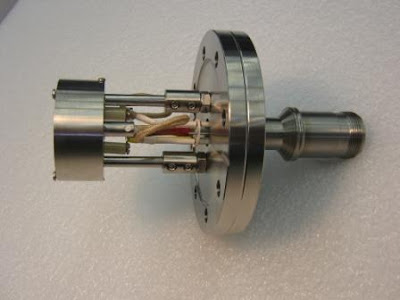
The inconel substrate heater is an essential part of some specific kinds of vapor deposition processes such as thermal evaporation, chemical vapor deposition, reactive sputtering, pulsed laser deposition and some more. The heater is generally made oxygen compatible which is especially designed for thin layer oxide based vacuum applications and processes. The best thing about such heaters is that they deliver accurate temperature and uniformed heating during the process of vapor deposition.

The Method of Vapor Deposition:

It is a method in which a thin-film of anti-oxidant material is deposited that wouldn’t degrade other properties of the metal. There are basically two mainstream methods of vapor deposition which are physical method and chemical method. Physical deposition method is capable of using any material that can be coated on the metal part or tool and is more environment friendly than the chemical method. The main purpose of coating the part is to prevent galling and to save money by not buying new tools or parts.


Physical Vapor Deposition: Physical deposition is considered as better and harder coating solution to prevent corrosion and physical depreciation. It increases lubricity and enhances release. Here also, the inconel substrate heater is vital to proceed with some certain types of physical deposition processes. During the process, there’s no requirement of chemicals and degrading their properties. It is highly preferred due to the hardness and resistance that is achieved after deposition. Titanium and other compounds of it are popularly used as coating materials. There are some additional compounds of titanium which are preferably used in some processes where the color of metal is required. For instance, the dies and screws which look like they are made of brass, generally are made of titanium compound coated over the metallic surface.

Chemical vapor deposition: In this process, a chemical (in a gaseous state) is deposited over the metal part surface. The gas is delivered into the reaction chamber where inconel substrate heater heats it up at a specific temperature according to the requirement to perform chemical reaction. Later, the gas condenses and solidifies as a thin layer over the metal when it comes in contact with the metal part.

The materials which are used as coating sources are carbon fiber, monocrystalline, carbon nanotubes, silicon, and silicon germanium, etc. Vapor deposition is generally utilized to produce optical fibers, semi-conductors, synthetic diamonds and nano machines, etc.

Get the Reliable Quality of Inconel Substrate Heater for Reactive Deposition by the Best Company

The Inconel Substrate Heater for Reactive Deposition is an oxygen good warmer & heater intended for thin film oxide based procedures and vacuum applications, for example, pulsed laser deposition(PLD), responsive sputtering, compound vapor deposition(CVD), warm dissipation, and that's only the tip of the iceberg. With accuracy temperature control and warming consistency, these radiators are the ideal apparatus for affidavit of thin film materials. 

Applications 

• Vacuum Annealing, Doping, Catalytic Reaction 
• In-Situ Surface Science, R and D 
• Gas Sensor Temperature subordinate Characterization 
• Epitaxy of Oxides, Nitrides, Carbides, Metals 

Key Features 

• Working temperatures up to 850¬∞C 
• Perfect with responsive gases, for example, O2, NH3, SiH4, CH4 
• Vacuum similarity from 10-8 Torr to 10-1 Torr
• Oxidation, consumption, and compound safe inconel composite material 
• Warming component neckline for component assurance 

Specification 

• Greatest temperature of task up to 850¬∞C 
• Vacuum similarity 10-8-10-7Torr 
• Coordinated in-fabricated k-type temperature sensor thermocouple with expanded adaptable and protected thermocouple wires 
• Adaptable glass fiber protected wire conduits for fueling 
• Inconel neckline with tapped gaps for substrate clasping 
• Accessible sizes From 0.5‚Ä≥ to 6‚Ä≥ distance across 
• Predisposition ability 
• Exactness temperature 
• PID controlled power supply 110V-220V 
• Simple to Install 

Inconel Substrate Heater

Worked for accuracy temperature control and uniform warming, the Inconel Substrate Heater is the ideal device for an assortment of thin film applications. The oxidation and concoction safe metal combination warmer & heater is intended to achieve temperatures up to 850¬∞C. It is good with receptive sputtering, PLD, PVD, e-shaft, warm dissipation, PECVD, ALD, in UHV or dormant (Ar, N2, He, H2) and responsive O2, Ozone, CO2, C2H2, CH4, NH3, SiH4, H2O, air and metal-natural forerunners from weight 10E-1 Torr through high vacuum up to 10E-8 Torr. 

The temperature consistency is inside 5-10%. All substrate warmer & heater models accompany stainless steel shield/neckline with 6 x4-40 tapped gaps for test bracing. They have incorporated inbuilt K-type thermocouple (with 24‚Ä≥ inch long adaptable fiber glass protected links) mounted from posterior drawing closer close to the surface of the hot surface for precise temperature estimation. Radiator and thermocouple wires have two 36‚Ä≥ long glass fiber protected and adaptable conduits for warmer & heater power and temperature estimation, separately. 

Blue Wave's radiator's back plate has one 10-32 tapped gap in the inside for warmer & heater mounting. The Inconel Substrate Heater is the best and appropriate for doping, epitaxial development, synergist responses, in-situ surface science as a component of temperature, and strengthening of nitrides, oxides, carbides, amalgams, metals, graphene, precious stone, CNTs, and complex multicomponent and multilayer thin movies. It can likewise be utilized for gas sensor portrayal, temperature subordinate electrical estimation of gadgets at high temperature in air, vacuum or N2 atm.

In case you are searching for the best organization who provide you the excellent quality of Inconel Substrate Heater in an affordable rate, at the point you are on the right place. There is a company who offering the ideal quality of Inconel Substrate Heater. Or else you can search throughout the web for the best one which suits on your requirement and necessity.

The Change in CVD Diamond Production Technique in Decades!

The chemical vapor disposition (CVD) diamond advanced out of decades-old procedures created amid the 1950s. It is interesting to note that an idea that is in certainty decades old is to some degree still used in a modern procedure of diamond manufacturing.

A significant part of the engineered diamond industry relies on a procedure known as HPHT or high-pressure high-temperature process. In spite of the fact that this technique is viewed as the highly followed procedure for developing diamonds in the present business and still remains the essential assembling process, a decades-old process is as yet exist in the business for making a remarkable assortment of shapes and films which address the requirements of an interminable cluster of industries.

The procedure is known as the chemical vapor disposition which develops diamonds through the procedure of low pressure, a direct inverse strategy interestingly with HPHT. The low-pressure process was introduced and developed in the 1950s and still utilized today for numerous other current techniques that are developing around this deep-rooted idea came into existence long back.

The way toward the manufacturing of diamonds through the low-pressure procedure of deteriorating carbon along with CVD diamond coatings gives new chances to produce units of diamonds in various shapes and different characteristics that completely utilize capabilities of the diamond.


The significance of CVD process is that it can provide the same result of HPHT without the high pressures that are required during the HPHT procedure. The CVD procedure brings about delivering an immense range of diamonds which are essential for some designing applications through a low-pressure process. An interesting certainty about the CVD diamond is that in the meantime the low-pressure technique was being utilized; General Electric was building up the HPHT method effectively. The company attempted a few methods for creating the CVD diamond by means of the low-pressure technique. After some failed attempts, they left the idea and kept on developing diamonds through the HPHT method.

General Electric's endeavors at the low-pressure technique were being led before Union Carbide effectively finishing their trial attempt at low-pressure manufacturing. Following the victory by Union Carbide, Japanese researchers found a technique for developing diamonds at a quick pace through low-pressure procedures. This brought about a noteworthy achievement in the mass production of the CVD diamond and considered as a remarkable point for many diamond businesses in this industry. 

At first, it made numerous industries set unreasonable objectives for the diamond electronic items, however, the thought got on and other agencies started manufacturing the CVD jewel. The expanded accessibility developed the diamond electronics industry and also the demand for the CVD diamond kept on growing.

More than forty years after the fact developing CVD diamonds through the low-pressure process is as yet dynamic in making numerous items helpful to the advanced industry. The CVD diamond is currently entering another stage for development in a portion of its growing procedures that will give more consistency and fewer imperfections underway. This implies accomplishing more points of reference with respect to atomic fusion research and laser speed innovation through 50 years old idea.

5 Benefits of E-Beam Evaporation / Deposition Systems

Electron beam (e-beam) evaporation, also known as electron beam deposition, is the most versatile and commonly used technique for the p...