CVD Diamond Coating is Crucial to Building a Cutting Edge Technology!

CVD Diamonds are the ones that are synthetically produced through machines and used in many technical applications. These diamonds have a variety of use and are widely used in many niche markets. There are service providers who make or build these CVD Diamonds for various uses. The diamonds are utilized in the creation of optical, thermal, and modern technology. The diamond coating process consists of a matrix of poly and nano-crystalline diamond. It is grown on the surface of cutting tools in a vacuum coating process. It also increases the tool life and performance significantly in highly abrasive machining applications. 

Here are the Advantages of CVD Diamond Coating–

1.The varied crystal structures provide strong protection against abrasive and adhesive wear. The cutting-edge provides protection against mechanical shock.

2.The tool geometry is protected by the presence of pure diamond. It helps the designing of complex tools for specific applications.

3.The CVD Diamonds are manufactured in a cost-effective manner compared to real diamonds.

4.These Synthetic Diamonds are used for more resources and it is also easily accessible.

5.The diamond used on tools will have the highest degree of hardness and fracture toughness with the lowest coefficient of friction. It enables a longer tool life.

6.The diamond coated surfaces will produce the best finishes on machined parts.

7.The synthetic diamonds are considered as the hardest diamonds which have the highest thermal connectivity.


A hot Filament Chemical Vapor Deposition (HFCVD) reactor is used for diamond deposition with the use of a modified filament arrangement. The filament is mounted vertically with the drill held concentrically in between the filament coils, as opposed to the commonly used horizontal arrangement. It is a simple and inexpensive filament arrangement. The films are examined in terms of their growth rate, morphology, adhesion and cutting efficiency. Diamond coatings are grown atom by atom on the tool surface. Commercially various technologies are used to produce CVD Diamond tools.

CVD Diamond Tools and Tooling-

The CVD Diamond tooling applications are those where machining the material forms powder or small grit. Graphite or fiberglass are the perfect examples of diamond tooling and the primary operation at the cutting edge is basically abrasive wear rather than chip formation. The CVD diamond coating will last from 50 to 70 times longer than standard carbide. The diamond coating process is dependent on the selection of proper tool material.  A CVD diamond film is pure diamond and is made with a process called chemical vapor deposition. Diamond is composed of carbon atoms and when heated will absorb carbon to form carbides in the workpiece.

The life of a diamond-coated tool varies depending on the material being cut, the chosen feeds and speeds, and the geometry of the part. The machining function, the material, and the goals of the operations all must be considered on a case by case basis in order to provide a top performing CVD coated cutting tool. The quality of the tool grind is paramount to ensuring the strength of the tool’s cutting edge.

Know More about Hot Filament Chemical Vapor Deposition!

With across the board utilization of electronic gadgets the semiconductor business has seen a considerable measure of changes in fabricate of semiconductor gadgets. Out of numerous stages for semiconductor manufacturing, fabrication procedure is one of the most important steps. For fabrication of functional layers over a substrate, the most commonly used technique is CVD (Chemical vapor Deposition).

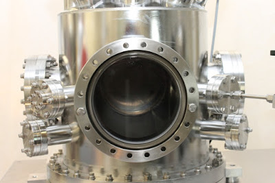
CVD is done in various processes. One of them is HFCVD (Hot Filament Chemical Vapor Deposition). The Blue Wave hot filament chemical vapor deposition system was built to produce concentrated, dense, adherent and coherent poly-crystalline diamond films on silicon, metallic and ceramic substrates. The Hot Filament Chemical Vapor Deposition HFCVD mechanism is beneficial as it gives the poly-crystalline stores of significant uniform miniaturized scale structure. It can be scaled for creation or extensive territory statement at bring down cost.


To improve the deposition parameters of diamond films, the pressure, temperature and distance between the filament and the susceptor should be considered. In any case, it is hard to exactly gauge and foresee the fiber and susceptor temperature in connection to the connected power in a hot filament chemical vapor deposition (HF-CVD) framework. The machine is intended to store different types of jewel coatings (UNCD-ultra nano crystalline diamond, NCD-nano crystalline diamond) poly-crystalline diamond movies and 2D carbon-that is graphene, which have wide use in electronic industry.

Equipment specifications:

  • This product has various fruitful features, which are mentioned below:
  • Specially designed substrate heater to attain a maximum temperature of 800 C, with a facility for rotational capacity of 20 RPM for the substrate and vertical movement of 20-80 mm.
  • A unique gas distribution system with mass flow controllers and bellow-sealed valves to ensure a controllable feed for deposition of mixed gases like methane, oxygen, acetylene and hydrogen.
  • An extraordinarily designed-filament holder gathering made of molybdenum, with numerous Tungsten wires working with a LT control supply for warming up the gases.
  • A state of the art PC-based control system with PLC or Lab View software, for total automatic system.
  • A molybdenum holder, with biasing capability.
  • A unique design of the sample holder, load lock transfer, and gas shower to provide proper distribution of gases for plasma generation and decomposition of the gases in the heated reactor area.
  • An appropriate pump-based vacuum system to create a high vacuum level as well as maintain adequate process pressure with an automatic throttle-valve. Process pressure is monitored by a capacitance mono-meter for accurate pressure control.


Chemical vapor deposition is another method of making metal objects more resistant to wear and friction and longer lasting. In this method, a chemical is deposited over the metal work surface in a gaseous state. Gases are delivered into the reaction chamber at specific temperatures required for the chemical reaction. The gases condense and solidify over the metal when they come in contact with it. The temperature of the metal is also very important. It affects the condensation of the gas over the metal. The apparatus used in this are the gas delivery system, the reaction chamber, energy source, vacuum system, process control equipment, exhaust system, exhaust treatment system and substrate loading mechanism.

By-products are also produced in the process. However, these can be removed gas flow in the reaction chamber. It is mostly used in microfabrication processes. The materials deposited are: silicon, carbon fiber, carbon nanotubes, silicon germanium, monocrystalline, etc. This method is used in producing synthetic diamonds, optical fibers, nano machines, semi-conductors, etc.

Get the Brief Information about Thin Film Deposition Control Service!

Thin Film Deposition is a vacuum innovation and technology for applying coatings of unadulterated materials to the surface of different objects. The coatings, likewise called films, are as a rule in the thickness scope of angstroms to microns and can be a solitary material, or can be numerous materials in a layered structure. This paper talks about the fundamental standards of thickness and rate control by utilization of quartz crystal observing.

One important class of deposition procedures is evaporation, which includes warming a strong material inside a high vacuum chamber, taking it to a temperature which creates some vapor weight. Inside the vacuum, even a generally low vapor weight is adequate to raise a vapor cloud inside the chamber. This vanished material consolidates on surfaces in the chamber as a covering or "film". This technique, including the general kind of chamber plans regularly utilized for it, is a brilliant possibility for effective control of rate and thickness using quartz precious crystals.


The key idea driving this sort of estimation and control is that an oscillator crystal can be reasonably mounted inside the vacuum chamber to get statement continuously and be influenced by it quantifiably. Particularly the wavering recurrence will drop as the precious stone's mass is expanded by the material being stored on it. To finish the estimation system, an electronic instrument constantly peruses the recurrence and performs fitting numerical capacities to change over that recurrence information to thickness information, both momentary rate and cumulated thickness. 

Such sensors and instruments are promptly financially accessible, incorporating into a coordinated bundle that not just peruses and shows the rate and thickness information, yet additionally gives yields to other deposition system components. It will have a simple drive signals to drive the source control supply in a closed loop procedure on the basis of rate information and accordingly can keep up a preset rate during deposition. What's more, it will have different yields to interface with capacities, for example, a source shutter triggered to close when the preset last thickness is accomplished. 

The first ramp up is generally slower and stops at some level just beneath vaporization and holds it to accomplish an adequate level of balance before making the second ramp up to vaporization. The last ought to in a perfect world be the real power level for the coveted testimony rate, and as a rule, since you will now devour material and covering the base of the shutter, this second ramp and soak is made genuinely short. However, those points of interest are client decisions. The controller gives you a chance to choose how you need it. 

While it is conceivable to utilize this same crystal observing and control innovation and technology in a sputtering system, it is entirely improved the situation a few reasons, one of which is that testimony rate versus cathode drive control is normally satisfactorily stable for process control in sputtering. Likewise, common sputter chambers are less manageable to situating crystals, and plasma can meddle with them.

Important Things to Know About CVD Diamond Coated Cutting Tool “Best of Breed” USA

CVD diamond coated cutting tools is playing a great role in growth and development. Driving this development is the utilization of composites inside the Automotive, Aerospace, and different ventures. In order to have a Best of Breed cutting tool used to machine (CFRP) Carbon Fiber Reinforced Plastic or distinctive composites, there must be a sensible cognizance of each application. The machining capacity, the material, and the objectives of the operations all must be considered on a case by case premise in order to give a best performing CVD covered cutting device. Since the cost of machining mistakes and rejecting material is exceptionally costly, a best performing tool is characterized as a tool only that last the longest, as well as a tool that performs with consistency. End clients don't anticipate the best case, yet the most exceedingly terrible, so a predictable wear rate notwithstanding stretched out wear is basic to giving a Best of Breed CVD diamond coated cutting tool.

The coating of cutting tools process with CVD diamond is an amazingly complex procedure with numerous factors that must be streamlined and firmly controlled in order to reliably deliver extended wear rates. At SP3 we have spent more than 100 man-years of R&D streamlining coating factors and growing tight process controls. Numerous of the key things that must be considered are:

Carbide

The carbide that is picked is imperative. SP3 is equipped for coating an assortment of carbides, both smaller scale grain and fine-grain, 6% cobalt carbides and at times 10% cobalt carbides. Contingent upon the application and tools geometry certain carbides will perform superior to others. SP3 has streamlined its procedures for particular carbides as every carbide responds to the coating procedure in an unexpected way.

CVD diamond


Tool Geometry

Tool design and configuration assumes a basic part in tool performance. We depend on the cutting tool producer's skill to give the best design, and the best assembling process for CVD coating. We do work intimately with our clients to test and upgrade tool design. We have best in class scientific tool in house to measure tool parameters, and the capacity to machine test tool in-house. 

Cutting Edge Preparation

The nature of the tool crush is fundamental to guaranteeing the quality of the tool's cutting edge. However, even with the best pound there can be edge defects and surface imperfections that can cause low mechanical quality bringing about premature edge chipping. This thus can fundamentally diminish the helpful existence of a cutting tool. How the cutting edge is prepared can likewise impact the nature of the diamond coating. Thus, SP3 has propelled tool in-house to perform examination of the cutting edge together with its clients. Furthermore, if the application requires, SP3 has the abilities to perform edge preparation as an extra piece of the assembling procedure. 

Substrate Preparation

With a specific end goal to accomplish perfect adhesion, which implies that the diamond coating basically wears through as opposed to chipping, flaking, or having the carbide break underneath the coating, the procedure parameters utilized for setting up the carbide are basic. There are two essential factors that must be firmly controlled in order to give perfect adhesion. In the first place is surface roughness, as the diamond bond to the tool substrate is a mechanical bond. The second factor is chemical compatibility. Cobalt, which is utilized as the binder for tungsten carbide, is an obstruction to diamond development. Cobalt must be expelled from the surface of the tool in a way that does not over debilitate the carbide. SP3 has exceptionally advanced procedures and controls inside its assembling operations that optimizes and tightly deals with the substrate preparation process. 

Diamond Coating

Diverse applications require distinctive coating thicknesses and attributes. At SP3 we have built up a wide assortment of 'recipe' that takes into consideration coating thicknesses from 3um up to 50um. What's more we can deliver extremely smooth coatings or rougher coatings, low stress coatings, compressive coatings, tensile coatings or pliable coatings, all tuned to the client's application. 

Diamond film coated by ultra hard materials is amazingly best and appropriate option for machining of aluminum alloys with the combination of high silicium substance and in addition graphite and carbon. Tests shows are incredible use of diamond coated tool in machining plastics, gold alloys and wood machining.

What Is Thin Film Coating And What Are Its Different Methods?

Thin film coating is the process of applying a very thin material onto a ‘substrate’ surface to be coated. It forms different layers and the coating comes through as the technological breakthrough for materials like electronic semiconductor devices or optical coating. Very thin layers of materials are used to develop filters and increase the insulation or conduction. It protects them from light or creates reflective surfaces. The thin films have a minimal thickness, ranging from fractions of a nanometer to several micrometers. Thus, this technology is preferred by a number of industries semiconductor industry, optical device industries, solar panels, and disk drives.


There are different parts in the deposition method which are listed as below–

• Conductive coatings
• Transparent coating
• Metallic coating
• Diamond 
• Dielectric thin film coating

There is a host of deposition services for manufacturers seeking to apply thin films, but the ideal method for a given application depends on the purpose of deposition, the surface makeup of the substrate, and the desired thickness. The thin film deposition is basically divided into 2 parts namely chemical or physical and further they have different classifications which will be discussed below.

Chemical Deposition

It is the process by which a substrate is fully submerged in a chemical fluid and then it is deposited onto the surface. It means that every surface of the substrate is coated equally. The most common types of chemical deposition are as follows –

Plating: In this process, a substrate is submerged in a chemical bath, often composed of water mixed with metal salts destined for deposition. They adhere to substrate in a uniform pattern, building up a thicker film. The substrate is connected to an anode powered by an external battery or rectifier.

Chemical Solution Deposition (CSD): It is a process which is similar to plating. But instead of metal salts in a water bath, organometallic powders in an organic solvent carry out the deposition procedure. CSD is cheaper and simpler than plating techniques.

Chemical Vapor Deposition (CVD): It involves a substrate placed in a pressurized chamber full of organometallic gas. The gas either reacts with the substrate surface or slowly dissolves over it, depositing the thin film evenly.

Physical Deposition

It is the technique which does not include chemical reaction and it relies on a mechanical or thermodynamic method for the production of thin films. It requires low-pressure environments for accurate and functional results.

The common types of physical deposition process are as follows–

Thermal Evaporation: In this, the deposition material is melted by an electric resistance heater until the surface of the substrate is covered. A variant of thermal evaporation uses an electron beam evaporator to melt materials on a substrate.

Sputtering: It occurs when a noble gas plasma is shot at a substrate in atom-sized particles. The impact of the particles triggers a collision cascade, which results in particle passing through the substrate.

Pulsed Laser Deposition: It involves a substrate and blocks film material in an ultra-high vacuum chamber. It bursts the light at the block of material which vaporizes and transfers to the substrate facing it.

How to Deposit a Thin Film of Materials Using PLD Technique?

In Pulsed Laser Deposition (PLD) technique, a high powered laser beam is focused inside a vacuum chamber. The material that needs to be deposited is kept inside the chamber and the process is also known as Physical Vapor Deposition (PVD). To melt, evaporate, and ionize material from the surface of a target, high power laser pulse is used. The technique is best used to deposit high-quality films of materials. In the presence of a background gases like oxygen, this process is incorporated. 


The technique is found much better than thin film deposition method. Listed below are the characteristics of PLD technique –

It enables the stoichiometric transfer of materials from target to substrate.The chemical composition of a complex material like YBCO is reproduced in the deposited film.The technique enables high deposition rates and the thickness can be enabled by simply turning on or off the laser.
  • The laser is used as an external energy source resulting in a clean process without filaments.
  • It occurs in both inert and reactive ground gases.
  • The process enables multilayer films to be deposited without the requirement.
Four Tips to Reduce the Cost of Your Custom R&D Deposition System

High film quality can be achieved with cost effective measures while choosing the conceptual phase of a coating system. The specifications for a thin-film coating should be best known for the overall requirement for a vacuum deposition system

Here are some suggestions for high-quality deposition system–

First, select the proper substrate size for the tool- The largest part of the cost in a deposition system is the maximum dimension of the substrate. Choose the smallest substrate size to minimize the system cost. It requires larger vacuum chambers along the large pumps and gate valves. 

Make sure that all the aspects of the deposition process are considered- Multiple monitoring devices are required within the chamber for complex coating. To evaluate the cost of a system, up-front planning becomes an important part.

Prepare and plan the facilities and the lab- Be ready for the system arrival and make advance planning for various system installations. 

Define the required throughput- The addition of a loadlock to an R&D tool can double the throughput for an incremental cost. Minimize the risks by having an entire production line down the line while replacing a key part.

The process of PLD is generally divided into different parts as–

• Laser absorption on the target surface
• Creation of plasma and laser ablation of the target material
• On the substrate, deposition of ablation material
• Dynamics of the plasma
• Nucleation of the film on the substrate surface

The high luminosity and transient nature of the plumes enable the temporary evolution of densities, temperatures, and velocities within the plasma. Different techniques used in the investigation of different stages of creation & creation are – Interferometry, Optical Spectroscopy and Laser-Induced Fluorescence (LIF). In the initial stages of the expansion, the plume emits high intensity broadband emission for saturating the detector.  

Develop Semiconductor devices with Thin Film Coating!

A thin film is controlling the synthesis of materials which is the fundamental thing in every material. The thickness of the film can range from a monolayer to micrometers. Thin film coating comes as the technological breakthrough for materials like electronic semiconductor devices or optical coating. A stack of thin films is called a multilayer and it plays a unique role in the development of materials with a unique property. Thin film deposition mainly refers to the technique of depositing a thin film of material onto a substrate.

Thin film deposition services assist the creation of new products in line with the customer requirements. With proper utilization of the resources, processing needs can also be customized. There are companies specializing in metalizing unique substrates which include all types of polyesters, polyolefins, wovens and fiberglass fabrics. There are various types of deposition methods like conductive coatings, transparent coating, metallic coating, diamond and dielectric thin film coating. Applications made out of the deposition are sensors, transistors, capacitors, solar cells and Wide band gap electronics. There are companies that are providing quality production, ideal for prototyping and users can get the contacts of many such companies online.

Read Also:- Diamond Lights up the Execution of Electronic Gadgets!
With the introduction of thin film coating and deposition services, there has been a tremendous technological impact affecting the lives of people. High performances computer, cameras, and storage devices are made of thin film coating. But researchers are again into innovating thin film deposition tools addressing their requirements and customizing the chemical vapor deposition tool. Companies are into the design of designing tools yielding high performance in nanotechnology, semiconductors and thin films.

Appropriate technique needs to be used for each application while using various thin film collating methods. Some of the capabilities are listed below –

Ion Plating: It increases the coating adhesion to the substrate and the substrate is electrically biased. It helps mold the physical characteristics of the coating deposit.
Sputtering: This type of coating method produces stream of coating atoms which has high adhesion to substrates.
Electron Beam: This type of film coating results in high deposition rates.
Reactive Sputtering: Sputtered coating like titanium nitride and alluminium oxide can be yielded through controlled sputtering atmosphere.

Using multi-purpose vacuum thin film deposition setup, thin films and coating are deposited. There are companies working on technological advancements of thin film deposition and coating. Companies manufacture high vacuum thin film deposition technology where thin film coating is added to the substrate. Total spectrum of vacuum deposition technology is offered ranging from evaporation, sputtering to the advancement of technology.

Get company contacts online specializing the manufacturing of deposition system for semiconductor R&D, device fabrication and provides quality thin film development services to their clients. To help create the future of thin film technology, companies need to focus on fabricating equipment and then devising the technology. Companies like Blue Wave Semiconductors are leading in the thin film deposition services with products like substrate heaters, deposition services, deposition accessories, and systems. Get innovative processing tools and material to the R&D customers and industrial partners.


5 Benefits of E-Beam Evaporation / Deposition Systems

Electron beam (e-beam) evaporation, also known as electron beam deposition, is the most versatile and commonly used technique for the p...